Atomic Layer Deposition – deposition of very thin layers of SiO2, Al2O3, TiO2, HfO2 and ZnO with good coverage of the vertical edges and perfect homogeneity.
Deep Reactive Ion Etching – etching of deep trenches and holes with high aspect ratio. Shallow silicon, SiO2, Al2O3 TiO2, HfO2, ZnO etching. Photoresist etching and surface activation.
Direct-write optical lithography – photoresist exposition without the need of mask with 600 nm resolution. Layout definition of the electronic devices, optical waveguides and sensors.
Inkjet priting technique – selective deposition of conductors (Ag nanoparticle, PEDOT:PSS based inks), dielectrics (SU8, PVP based inks), semiconductors (ZnO, PANI based inks) and seed layers (eg. diamond and ZnO)
Spin coating
Evaporation
High energy pulsed light curing, sintering or annealing – delivering up to 2500 J/pulse, radiant pulse energy up to 7 J.cm-2, pulse range from 100 to 6000 μs
UV ozone cleaning – up to 150 °C
High temperature annealing
Doctor blade applicator
Diagnostics
AC and DC electrical characterization – I-V, C-V, impedance (78 to 690 K)
Thin film resistivity measurement – van der Pauw (VDP) method, four point probe (4PP) method
Deep level transient spectroscopy (DLTS) – up to 690 K
Hall-effect measurements
Standard electrical and magneto-electrical transport measurements – temperature range 10-350K
Optical characterization – photoluminescence, photoconductance and photoreflectance in the UV/VIS range
Gas sensor measurements – response/recovery time, stability, reproducibility, repeatability, reversibility, selectivity etc.
Optical power measurement
m-line spectroscopy
Raman spectroscopy characterization – surface characterization using three different laser wavelengths. Analysis of the chemical composition Surface 2D mapping and depth profiling. Lasers 532 nm, 633 nm and 830 nm, temperatures from 78 to 690 K.
CoventorWare (overview.pdf) is an integrated suite of design and simulation software that has the accuracy, capacity, and speed to address real-world MEMS designs.
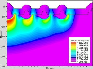
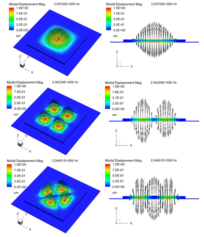
The included field solvers provide comprehensive coverage of MEMS-specific multi-physics, such as electrostatics, coupled electro-mechanics, piezoelectric, piezoresistive, and damping effects.
Common MEMS simulations, including:
Coupled electromechanical (ex. Pull-in, electrostatic spring softening)
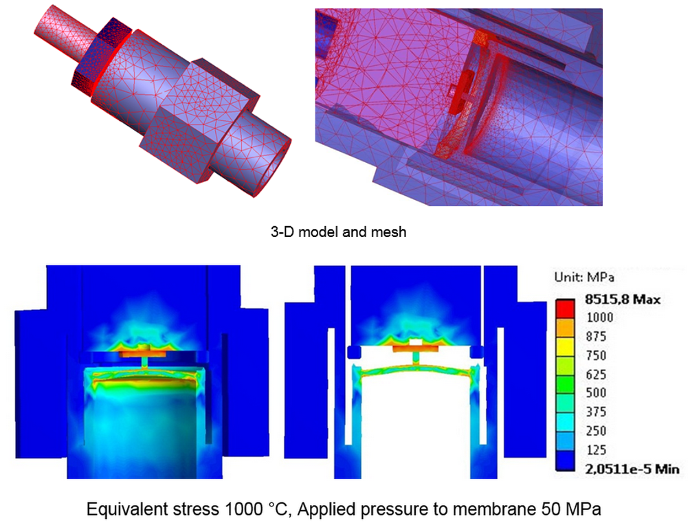
ANSYS Workbench is a software environment for performing structural, thermal, and electromagnetic analyses.
RSoft
The RSoft Photonic Component Design Suite allows users to design and simulate passive photonic devices for optical communications, optoelectronics, and semiconductor manufacturing (rsoft.pdf, allinone.pdf).
MOST – An iterative design and optimization utility for all of the RSoft passive device design tools (Most.pdf)
OPTICAD
OptiCAD is a computer program for the layout and analysis of 3D optical systems.
Components include spherical and cylindrical lenses; conical, parabolic, elliptical, spherical, and flat mirrors; full (closed) cylinders and ellipsoids; transmitting and reflecting rods; parabolic and elliptical trougs; single- and double-sided reflective surfaces; apertures of finite extent; lightpipes; multiple sources and detectors; compound parabolic concentrators; Fresnel lenses; and polygonally faceted objects – OptiCAD.pdf